
← Industries
INDUSTRY
Electronics & Semiconductor Industry
As component sizes shrink, inspection resolution and repeatability become decisive. Micron-scale defects require the right combination of high-resolution camera and lens.
Typical applications
- PCB placement and solder inspection
- Micro-component presence and position verification
- Wafer and die surface defect detection
- Reading of small 2D codes
Related product groups
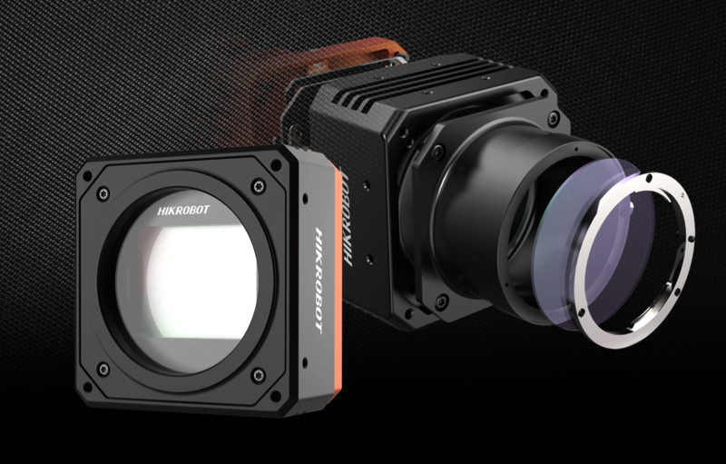
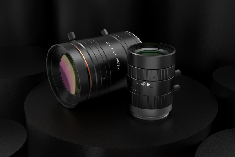
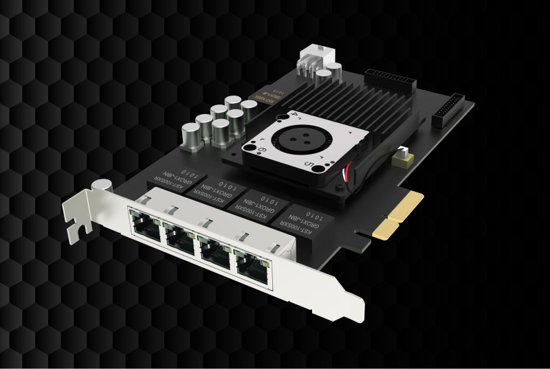
Let’s define the application on your line together
We select the right camera, sensor and lighting for your product, line speed and operating conditions, and run a pre-test on samples where needed. Contact us →